


Semiconductor Radiation Detectors Designed for Extreme Environments
A series of new progresses in developing of semiconductor-based radiation detectors have been achieved at the Institute of Nuclear Energy Safety Technology (INEST), Hefei Institutes of Physical Science, Chinese Academy of Sciences, by collaborating with Nanjing University, the University of Science and Technology of China, the Institute of Modern Physics Chinese Academy of Sciences, and Nanhua University. Representative achievements have been published in well-known journals including IEEE Electron Device Letters and Nuclear Instruments and Methods in Physics Research A.
Radiation detectors serve as the "eyes" for humans to observe and study nuclear radiation and microscopic particles, which is playing an irreplaceable role in basic research, nuclear energy development, and nuclear technology applications. However, the widely used detectors currently face issues such as low sensitivity or insufficient environmental adaptability, making them unsuitable for applications in high-temperature and high-radiation environments. In contrast, semiconductor-based radiation detectors using wide-bandgap and ultra-wide-bandgap materials offer many advantages, such as high-temperature resistance, radiation hardness, and easy integration. This has become an important development direction in advanced radiation detection technology in recent years.
Based on wide-bandgap and ultra-wide-bandgap materials, researchers at INEST have optimized the design, fabrication process, and testing schemes of semiconductor-based radiation detectors to address the issues of current detector techniques. These efforts have significantly improved the performance of radiation detectors, and lead to a series of research achievements.
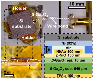
Figure 1: The optical microscope image and structural schematic diagram of the Ga2O3 detector
The researchers have fabricated large-area p-NiO/β-Ga2O3 devices with low interface state density and leakage current levels, and coupled them with boron-based neutron conversion materials. The detector achieved a neutron detection efficiency close to 1% and completed the first experimental verification of Ga2O3-based thermal neutron detector. This work has made a valuable contribution to the development of neutron detection technology for applications in extreme environmental conditions.
A 4H-SiC Schottky barrier diode (SBD) detector system has been fabricated with ultra-low doping concentration (<1×10¹⁴ cm⁻³) and ultra-thick epitaxial layers (80 μm). The detector exhibits excellent linear response and an energy resolution of 1%, enabling complete energy deposition for 12 MeV high-energy α particles. The detector can continuous operation stably at 80°C for long periods (24 days), providing strong technical support for accurate measurements of superheavy elements under extreme conditions.
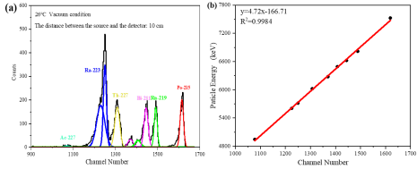
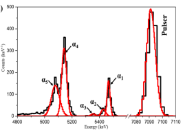
Figure 3: Pulse height spectrum obtained by a 4H-SiC detector with NO annealing aftertreatment progress technique under irradiation of a 239Pu-241Am hybrid source
The oxygen-nitrogen (NO) annealing process has been developed to improve the SiC/SiO₂ interface, enhancing the detector performance and achieving a high α-particle energy resolution (better than 5‰ @ 5486 keV). Additionally, a novel thermal neutron detector based on a boron neutron conversion layer has been developed, successfully distinguishing the two primary reaction channels of thermal neutrons and boron nuclear reactions, which completed the principal verification of this novel detector for neutron detection.
The above-mentioned researches were supported by the National Major Scientific Instrument Development Project, National Key Research and Development Program, Anhui Province Key Research and Development Program, and the Open Fund of the Key Laboratory of Advanced Nuclear Energy Technology Design and Safety, Ministry of Education.
Article link:
https://doi.org/10.1109/LED.2024.3522482;
https://doi.org/10.1016/j.nima.2024.169683;